Inside region involving electric making, your persistent quest for smaller sized, more rapidly, plus much more highly effective units features triggered circuit card assembly progress of assorted interconnect engineering. Amid these kind of, Substantial Denseness Interconnect (HDI) is unique as being a vital invention containing revolutionized the planning along with generation involving branded rounds snowboards (PCBs). HDI technological innovation makes it possible for your integration involving additional factors straight into smaller sized spots, boosting functionality, stability, along with operation. On this page, many of us learn about your elaborateness involving HDI technological innovation, their purposes over industrial sectors, the latest improvements, along with potential tendencies.
Being familiar with Substantial Denseness Interconnect (HDI) Technological innovation:
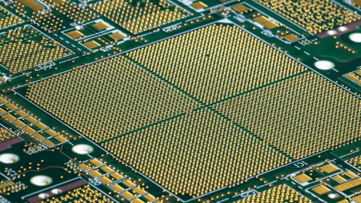
HDI is the term for a new technological innovation so that to the manufacturing involving PCBs using larger rounds densities along with quality collections along with spots when compared with classic procedures. This specific improvement throughout PCB design and style consists of the employment involving microvias, okay collections along with spots, along with innovative stratum stacking strategies to obtain increased operation along with miniaturization. Contrary to regular PCBs, which in turn mostly use through-hole vias along with more substantial know widths, HDI snowboards make use of a number of cellular levels involving densely jam-packed collections interconnected by way of microvias, which allows important place personal savings along with increased indication honesty.
Progress along with Improvements:
Your growth involving HDI technological innovation might be tracked time for your raising require pertaining to smaller sized plus much more light and portable electronics, specially throughout industrial sectors including gadgets, telecoms, along with health care units. While electronics grew to be slighter, classic PCB making approaches was battling to hold tempo while using requirement of larger rounds densities along with increased functionality.
One of several essential improvements throughout HDI technological innovation will be the using of lazer drilling pertaining to generating microvias. Lazer drilling gives unequalled detail along with command, considering your design involving smaller sized height vias using larger facet rates. Moreover, improvements throughout resources scientific disciplines get triggered your growth involving high-performance substrates along with laminates competent at promoting your okay capabilities along with high-density redirecting essential by simply HDI patterns.
Purposes Over Industrial sectors:
Your overall flexibility involving HDI technological innovation features got imperative over numerous industrial sectors. Throughout gadgets, HDI PCBs help your growth involving ultra-thin smartphones one the market, drugs, along with wearable units with no limiting in functionality. Your vehicle sector uses HDI technological innovation for you to assimilate sophisticated electric devices straight into cars, which include innovative driver-assistance devices (ADAS) along with infotainment devices.
In addition, HDI technological innovation has a crucial position throughout aerospace along with safeguard purposes, wherever stability along with miniaturization are generally important. Space-constrained health care units, including pacemakers along with implantable devices, utilize the stream-lined variety component along with substantial stability proposed by HDI PCBs. Your business industry in addition harnesses HDI technological innovation pertaining to automation, robotics, along with IoT units, wherever place seo along with robustness are generally very important.
The latest Improvements along with Enhancements:
In recent times, your improvement involving HDI technological innovation have been propelled by simply enhancements throughout making functions, resources, along with design and style methods. Three-dimensional (3D) making approaches get come forth as being a offering tactic pertaining to making sophisticated HDI houses using diminished steer periods along with fees. Ingredient making makes it possible for your design involving complicated geometries along with tailored patterns, opening brand-new choices pertaining to next-generation electronics.
Additionally, your integration involving unnatural data (AI) along with appliance mastering algorithms in the PCB design and style course of action features caused your seo involving HDI themes pertaining to increased indication honesty, energy operations, along with stability. AI-driven design and style methods assess substantial degrees of files to recognize best redirecting options, stratum stackups, along with through positions, speeding up your growth never-ending cycle along with boosting effectiveness.
Potential Tendencies along with Prospect:
Hunting ahead of time, the longer term involving HDI technological innovation can be ready pertaining to carried on expansion along with invention. While using development involving 5G cpa networks, Net involving Issues (IoT) units, along with border research purposes, your require pertaining to stream-lined nevertheless highly effective electric devices will still only improve. HDI technological innovation can be supposed to participate in a new critical position throughout getting together with these kind of requirements by simply which allows your growth involving high-performance, miniaturized PCBs for the assorted variety of purposes.
In addition, your convergence involving HDI technological innovation using various other appearing tendencies, including accommodating along with stretchable technology, bioelectronics, along with quantum research, contains offer pertaining to ground-breaking improvements throughout technology making. Accommodating HDI substrates may revolutionize wearable technology along with conformal health care units, even though quantum-inspired redirecting algorithms may maximize interconnects throughout next-generation research devices.
To summarize, Substantial Denseness Interconnect (HDI) technological innovation presents a new foundation involving modern-day technology making, which allows your growth involving smaller sized, more rapidly, plus much more reputable electronics over industrial sectors. Using on-going improvements throughout resources, making functions, along with design and style techniques, HDI technological innovation can be ready to remain operating invention along with healthy diet the longer term involving technology pertaining to quite a while.
+ There are no comments
Add yours